Sample and Hold
Sample and hold circuit is the first step in the process of analog to digital conversion. It actually takes samples of the analog signal at specific time intervals depending on the clock frequency. Clock frequency is the frequency at which we are taking samples of the analog signal. Basically sample and hold process comprises of two steps:
- Take samples
- Holding samples
Samples are taken at the clock frequency while the hold step is accomplished by connecting the capacitor in the parallel to the output of the sampled signal. The simple sample and hold circuit is given below
The switch is on whenever we want to take sample and capacitor helps to hold that sample. Practrically the switch is implemented by connecting the fast switching FET switch, and samples are taken on some clock frequency which can be implemented by any timer circuit. The capacitor is invariably discharged by its own leakage current.
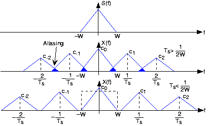
In our project we are taking audio signal frequency as the input signal. for sampling the input signal we must have sampling frequency twice of the bandwidth of the input signal. This is given by the sampling theorem. This theorem states that the sampling frequency must be the twice of the bandwidth of the input signal. If the sampling frequency is below the twice of the input signal bandwidth then aliasing of the samples will occur. Aliasing refers to an effect that causes different signals to become indistinguishable when sampled. The aliasing if the samples can be observe by taking the Fourier transform of the samples or by viewing the samples in the frequency domain. The higher the sample rate the more accurate the analog information will be in digital form and so the bandwidth. The higher sample rate has higher accuracy. The aliasing of the samples are describes in the figure given below
Components used in the project are as following:-
JFET BF245C:
The JFET BF245C is the simplest type of field effect transistor. It can be used as an
electronically-controlled switch or as a voltage-controlled resistance. Electric charge flows through a semiconducting channel between “source” and “drain” terminals. By applying a bias voltage to a “gate” terminal, the channel is “pinched”, so that the electric current is impeded or switched off completely.
Diode
Capacitors
Resistance
Power Supply
Function Generator:
The sampling clock is given to the gate channel of the JFET by the function generator or any timer circuit. The sampling frequency has its limitation which is describe by the sampling theorem.
Output waveform:
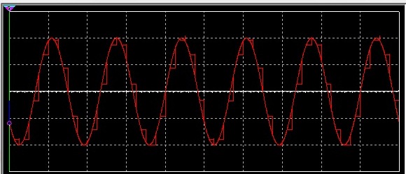
The output waveform of the simulation of sample and hold circuit is given below:
To download the circuit diagram click the link given below
Download attachment
 BooknStuff Find educational solution, notes and support for various standards


nice work.. this project is amazing.. keep up the good work..